When a photon interacts with a semiconducting material, it can pass completely through the material, or it can be reflected away from the incident surface, or it can be absorbed in the bulk of the material. Photon absorption can occur when the photon’s energy coincides with the semiconductor’s bandgap energy. In this case, when the photon with energy \(E_g\) strikes a valence electron with energy close to \(E_V\), the electron can absorb the photon’s energy thereby boosting its own energy level up to \(E_C\), resulting in the generation of a mobile electron/hole pair. If the photon has energy less than \(E_g\), then the electron is unable to absorb it since the combined energy would place it in the fobidden gap, so the photon passes through unabsorbed. Photons with energy above \(E_g\) can be absorbed, but with increasing energy they are much more likely to be absorbed or reflected near the material surface rather than in the bulk.
Optoelectronic interactions have several important applications. The simplest is the photo resistor: when many photons are absorbed, the mobile charge concentration increases, causing increased conductivity in the material. This phenomenon can be used in basic circuits that respond to bright sources such as sunlight or lasers. Beyond the photoresistor, there are many more sophisticated applications which all rely on junction physics, especially the physics of the depletion region. These applications include solar cells, photodiodes, digital cameras, LEDs and lasers, among others. To understand these, we’ll begin with a close look at the junction.
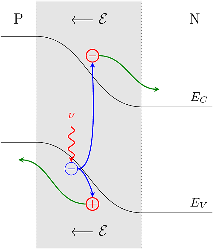
When a photon is absorbed in the quasi-neutral bulk regions of a PN diode, it adds to the pool of mobile carriers and slightly alters the conductivity, which is a fairly weak interaction and not much happens. When a photon is absorbed in the depletion region, the result is more interesting: a new pair of mobile carriers is generated, which are immediately swept apart by the electric field, setting up a net reverse current through the junction. This current is called the photo current, and is directly proportional to the rate of photon absorption in the depletion region.
The process of photon absorption is illustrated in the figure below. A photon (identified by the Greek symbol \(\nu\)) is absorbed by an \(e^-\) in the valence band. As a result, the \(e^-\) is promoted to the conduction band, leaving behind a mobile \(h^+\). The opposite-charged \(h^+\) and \(e^-\) are accelerated away from each other by the built-in \(\mathcal{E}\)-field, resulting in a photocurrent. On each side of the junction, we see the flow of one charge carrier per absorbed photon.
Each photon arrives with an energy of \(hc/\lambda\) [Joules], equivalent to \(\frac{hc}{q\lambda}\,\text{eV}\). Since the electron must bridge the bandgap, any absorbed photons must have energy greater than \(E_g\).
Optoelectronic devices are usually specified in radiometric units. The photon flux \(\Phi\) is defined as the rate of photons of a particular wavelength passing through a material section, usually with units of photons/s\(\,\text{cm}^2\). As illustrated in the figure below, photons incident on the surface plane are “eligible” to be absorbed as they pass through the bulk.
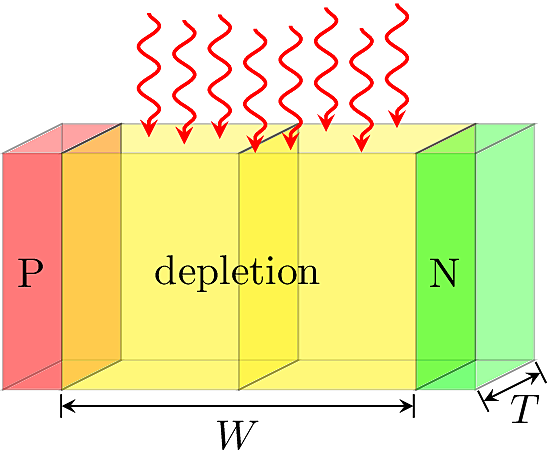
If the junction thickness is \(T\) and the depletion width is \(W\), then the photocurrent should be
\[I_{\rm ph} = q\eta \Phi TW,\]
where \(\eta\) is a wavelength-dependant scale constant called the quantum efficiency that indicates the probability of a photon being absorbed before passing all the way through the material. The underlying physics lumped into \(\eta\) can be complex: smaller wavelengths (in the blue or ultraviolet range) have higher energies and are more likely to be reflected or absorbed near the material surface. Larger wavelengths have lower energies (in the red or infra-red range) and tend to penetrate deeper and may pass all the way through without being absorbed. In addition, recombination of \(e^-\)/\(h^+\) pairs may occur within the material, causing a portion of charge carriers to annihilate before they cross the junction.
The photo current is commonly expressed as a function of the total radiant flux \(\phi\), defined as the total optical power incident upon the material’s surface, with units of Watts. The irradiance \(E\) is the radiant flux per unit area. These terms and their relationships are summarized in the table below.
| Quantity | Symbol | Units | Definition |
|---|---|---|---|
| Quantity | Symbol | Units | Definition |
| radiant flux | \(\phi\) | W | total optical power on surface |
| photon flux | \(\Phi\) | photons/s\(\,\text{cm}^2\) | density of photons per second |
| quantum efficiency | \(\eta\) | fraction of photons absorbed | |
| irradiance | \(E\) | W/\(\,\text{cm}^2\) | power density on surface |
| photocurrent | \(I_{\text{ph}}\) | A | current induced by absorbed photons |
| photon energy | \(e_{\text{ph}}\) | J | energy of a photon \(e_{\text{ph}}=hc/\lambda\) |
\(\phi\) |
\(\Phi\) |
\(E\) |
|
|---|---|---|---|
\(\phi\) |
\(\Phi\) |
\(E\) |
|
\(\phi=\) |
\(\Phi e_{\text{ph}}WT = \frac{\Phi TW hc}{\lambda}\) |
\(EWT\) |
|
\(\Phi=\) |
\(\frac{\phi}{WT e_{\text{ph}}}=\phi \frac{\lambda}{hcWT}\) |
\(\frac{E\lambda}{hc}\) |
|
\(E=\) |
\(\frac{\phi}{WT}\) |
\(\frac{\Phi hc}{\lambda}\) |
|
\(I_{\text{ph}}=\) |
\(\frac{q\eta\phi\lambda}{hc}\) |
\(q\eta \Phi TW\) |
\(\frac{q\eta E\lambda WT}{hc}\) |
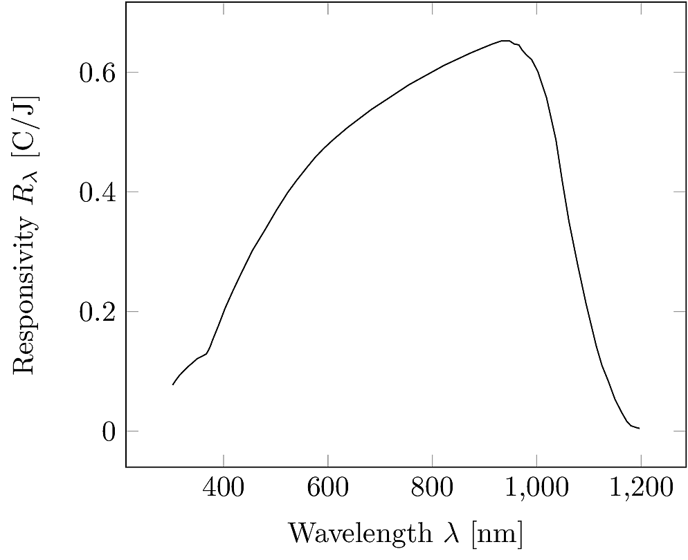
where \(h\) is Planck’s constant, \(c\) is the speed of light and \(\lambda\) is the photons’ wavelength. The photocurrent is also commonly expressed as
\[I_{\rm ph} = R_\lambda \phi\]
where \(R_\lambda\) is the material’s spectral responsivity with units A/W (equivalently Coulomb per Joule), given by
\[R_\lambda = \frac{q\lambda\eta}{hc}.\]
From these relationships, we can draw a few important observations:
The photocurrent is proportional to the depletion width \(W\), so for a good photodetector we need to maximize the depletion region. This means we need very weak doping on one side of the junction, since \(W\propto \left(\frac{1}{N_A}+\frac{1}{N_D}\right)^{1/2}\).
The responsivity is proportional to the photon wavelength \(\lambda\), which is larger toward the infrared end of the spectrum, and smaller toward the blue and ultraviolet end. This means we should expect a weaker response for blue, violet, and ultraviolet wavelengths.
The responsivity also depends on \(\eta\), which is a function of wavelength. At larger wavelengths (infrared), \(\eta\) tends to decrease since the low-energy photons pass through without being absorbed. At small wavelengths (blue), most photons are reflected away at the surface, so \(\eta\) decreases again.
In order to be absorbed, the photon energy must exceed the material’s bandgap. For Silicon, the bandgap energy is \(E_G=1.12\,\text{eV}\). This corresponds to a maximum wavelength of about 1,100nm.
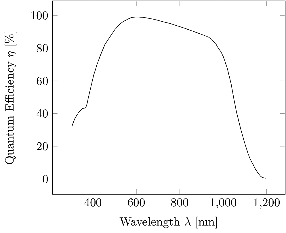
When the quantum efficiency is multiplied with the wavelength to get responsivity, the result is that \(R_\lambda\) tends to peak at a wavelength a little below the bandgap limit. For Silicon photodiodes, this is usually in the vicinity of 900nm:
A basic photodetector circuit based on a PN junction is shown below. The diode symbol has two arrows pointing inward, indicating that it is intended for use as a photodiode. The diode is held in reverse bias for two reasons:
Reverse bias maximizes the depletion width, and consequently improves photon collection
The reverse-bias current is approximately equal to the photocurrent, which is directly proportional to the collected light.
The photocurrent is measured by monitoring the voltage drop across resistor \(R\). The output voltage should be \(v_{\text{out}}=V_{\text{DD}}-I_{\text{ph}}R\).
This circuit is also called a pixel sensor, and is a linear photodetector. Linear detectors are not necessarily the best option for all applications. Considering that the difference in irradiance between outdoor and indoor lighting can span four orders of magnitude, it is not feasible to design a passive linear photodetector for general use.
An alternative design is the active pixel sensor (APS) shown in the figure below. In this design, a MOSFET (\(M_1\)) is first switched ON to pull node \(v_x\) up to \(V_{\text{DD}}-{V_{\text{Th}}}\), placing the diode in reverse bias. Then \(M_1\) is switched OFF, leaving \(v_x\) floating on the parasitic capacitor \(C_P\) (in every node, there is always an implicit parasitic capacitance due to the surrounding materials; in this circuit we made it explicit). The photocurrent slowly discharges \(C_P\), causing \(v_x\) to drop in proportion to the time integral of \(I_{\rm ph}\). The output voltage is isolated by a source-follower (\(M_2\)).
Considering the APS circuit shown above, suppose \(M_1\) is turned OFF at time \(t=0\), and the signal at \(v_\text{OUT}\) is sampled after a short time \(\Delta t\). Then the change in output voltage should be
\[\Delta v_\text{OUT}= -\frac{1}{C_P}\int_0^{\Delta t} I_{\rm ph} dt.\]
If the sampling time is very small so that \(I_{\rm ph}\) is nearly constant, then the expression simplifies to
\[\Delta v_\text{OUT}= -\frac{I_{\rm ph} \Delta t}{C_P}.\]
The detector’s sensitivity is therefore a function of \(\Delta t\), which can be adjusted digitally using a clock divider circuit. If \(v_\text{OUT}\) is saturated, meaning \(C_P\) is fully discharged during the sampling interval, then the measurement can be repeated with a smaller \(\Delta t\). This gives APS cameras the ability to adapt to a wide variety of lighting conditions without depending on mechanical accessories. In low-light conditions, the sensitivity of APS circuits is limited by the diode’s reverse leakage current, which in this context is called the dark current. It is also limited by sources of noise within the photodiode and its surrounding circuit.
Since the photocurrent only responds to photons collected within the depletion region, to make a sensitive photodetector we should make \(W\) as large as possible. Recall the expression for \(W\) in reverse bias:
\[W = \sqrt{\frac{2\epsilon}{q}\left(\frac{1}{N_A} + \frac{1}{N_D}\right) \left(V_0+V_R\right)}.\]
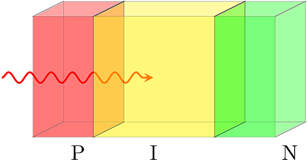
We see that \(W\propto \sqrt{1/N_A + 1/N_D}\). Suppose we let \(N_A\) or \(N_D\) go to zero. In that extreme limit, \(W\) goes to infinity, so the weakly doped side of the junction will be fully depleted throughout its volume. By placing an undoped region of intrinsic semiconductor in between the P and N regions of a normal diode, a very wide depletion zone is created, resulting in a highly sensitive photodetector. The wide depletion width also reduces the junction capacitance and gives it a high-bandwidth in reverse bias, making for a fast photodetector. A couple of common PIN diode structures are shown in the figures below.
PIN photodiodes respond very quickly, and can be used in high-speed optical data links. Their quantum efficiencies can exceed 90%. Their wavelength response depends strongly on their material composition, and Silicon is often not the best choice. In fiber optic cables, optimal transmission is achieved for a wavelength of 1550nm, making this the world’s most widely used wavelength for telecommunication. PIN diodes made from Germanium or from alloys such as Indium-Gallium-Arsenide (InGaAs) have a good response in this region, since their bandgap energy is lower than the photonic energy at that wavelength. Silicon’s bandgap corresponds to a wavelength of about 1100nm, making it a poor detector for fiber optic applications. Si is still a relatively good detector for infrared and visible light, providing the basis for low-cost and high-resolution digital photoghraphy that is well integrated with other Si electronics.
The PIN diode is also interesting for RF applications. The low junction capacitance makes it very good for rejecting RF frequencies when reverse biased. When forward biased, the large depletion region tends to linearize the diode’s transfer characteristic at high frequencies, thereby reducing distortion. It can be used as a variable resistor, with the resistance tuned by the forward bias current. Since the small-signal resistance can be made very low, PIN diodes make high-quality RF switches. Their main limitation in this use is that they cannot be rapidly switched between ON and OFF states, due to the large charge stored in the intrinsic region.
If a photodiode is biased close to the edge of its reverse breakdown point, absorbed photons can provide enough energy to stimulate avalanche multiplication. This method can be used to create highly sensitive photon detectors used in scientific applications. In order to achieve a good gain, the junction must have a very large breakdown voltage and a large reverse bias (typically exceeding 100V. Single-photon sensitivity can also be achieved if the diode is biased slightly beyond its breakdown point, referred to as Geiger mode since the diode will emit short pulses of current in response to individual photons, much like a Geiger counter.
Light Emitting Diodes are like reverse photodetectors. When a mobile charge pair recombines in forward bias, a photon is emitted. The energy of this photon is set by the material’s bandgap \(E_g\). The first observation of photon emission from a semiconductor – a phenomenon called electroluminescence – was in 1907. Commercially viable LEDs with visible emission appeared in 1962, and a telecom-grade LED was first produced in 1976. The first commercial LEDs were made from a Gallium Arsenide (GaAs) alloy, which provides high electroluminescence due to its direct bandgap. We previously glossed over some of the physics governing energy band transitions. An electron’s energy level is a scalar quantity, but the transition is also affected by the electron’s momentum, which is a vector quantity.
In an indirect-bandgap material like Si, electrons cannot change energy levels unless they also change the direction of their momentum vector. A photon by itself cannot provide the needed change in momentum; that change has to come from a thermal interaction with the crystal lattice. At the quantum level, thermal fluctuations appear as quasi-particles called phonons. To reach the conduction band, a Si valence \(e^-\) needs to absorb a photon and have a precise phonon collision at the same time. For that reason, Si diodes dissipate most of their transition energy as heat. These are called non-radiative transitions since most of the energy goes into heat, but a small fraction of recombinations do yield photons, it’s just a very inefficient process.
Direct bandgap materials, on the other hand, can undergo energy level transitions without heat dissipation. This allows production of highly efficient bright light sources. Today LEDs are made from diverse materials and can emit light across the whole visible spectrum, ranging from infrared to ultraviolet. Various flourescent coatings have also been introduced to imitate the look and feel of incandescent lights, which has sped the adoption of LED-based lighting in homes and commercial buildings. LED lighting has also benefitted from advances in solid-state AC/DC conversion, which can now be done with efficiency above 99%. Thanks to microelectronic fabrication, these devices can all be integrated into a light-bulb sized package and used as an in-place upgrade for century-old lighting systems.
Another crucial application of LEDs is the laser. A typical LED undergoes a process of random recombination called spontaneous emission. Einstein discovered (mathematically) that the probability of recombination/emission is increases if another photon of the same energy is present. In this process, called stimulated emission, a photon induces a recombination event leading to a second photon emitted with the exact same wavelength, direction and phase as the original photon. Then there are two photons that can stimulate two more emission events, leading to something like avalanche multiplication of photons.
The idea of a diode laser is to put reflective surfaces on each side of an LED junction, so that more emission is continually stimulated by the reflected photons. A small hole is provided to allow a narrow column of photons to escape, creating a laser beam. Since some of the reflected photons are re-absorbed by the material, the device reaches a saturation level of photon emission. The LED laser is now the basis of optical storage media (e.g. CDs, DVDs, BlueRay discs), fiber optic transmitters, and numerous other applications in science, medicine and entertainment.
High-energy particles are produced by a variety of phenomena. X-rays and gamma rays are very high-energy photons that may be produced by radioactive decay or from cosmic sources. Other common radiation byproducts include alpha particles (high-energy helium nuclei with two protons and two neutrons), beta particles (high-energy electrons or positrons), and the high-energy collision byproducts produced in particle accelerators. There is also a constant rain of cosmic rays bringing high-energy photons from outer space.
All of these rays and particles interact with semiconductor junctions. As a high-energy particle passes through the material, it delivers ionization energy to a large number of charges. This is similar to photon absorption except a very large number of mobile charge pairs can be created along the particle’s path as it passes through the material. In a reverse biased PN junction, this creates a big current pulse with a slow decay due to the ongoing diffusion of carriers from the particle’s charge wake. These events cause single-event upsets in modern electronic devices, sometimes leading to serious errors or system failures.
Suitably designed PN junctions can be used as detectors for nuclear and subatomic particles. As an example application, at CERN’s Large Hadron Collider (LHC) facility, specialized pixel detector chips are arranged around the exterior of a tube. Protons are accelerated within the tube and smashed together at extremely high energies in order to break them into their constituent elementary particles. The collision byproducts are scattered out of the tube, passing through an array containing tens of millions of pixel detectors. The pixel detectors are fairly large by silicon standards – 50\(\mu\)m by 400\(\mu\)m – and are packaged in thin columns called “staves” containing several pixels each. The staves are layered in a ratchet-like orientation so that they can detect particles’ paths in three dimensions as they fly out of the collider.